Design Images
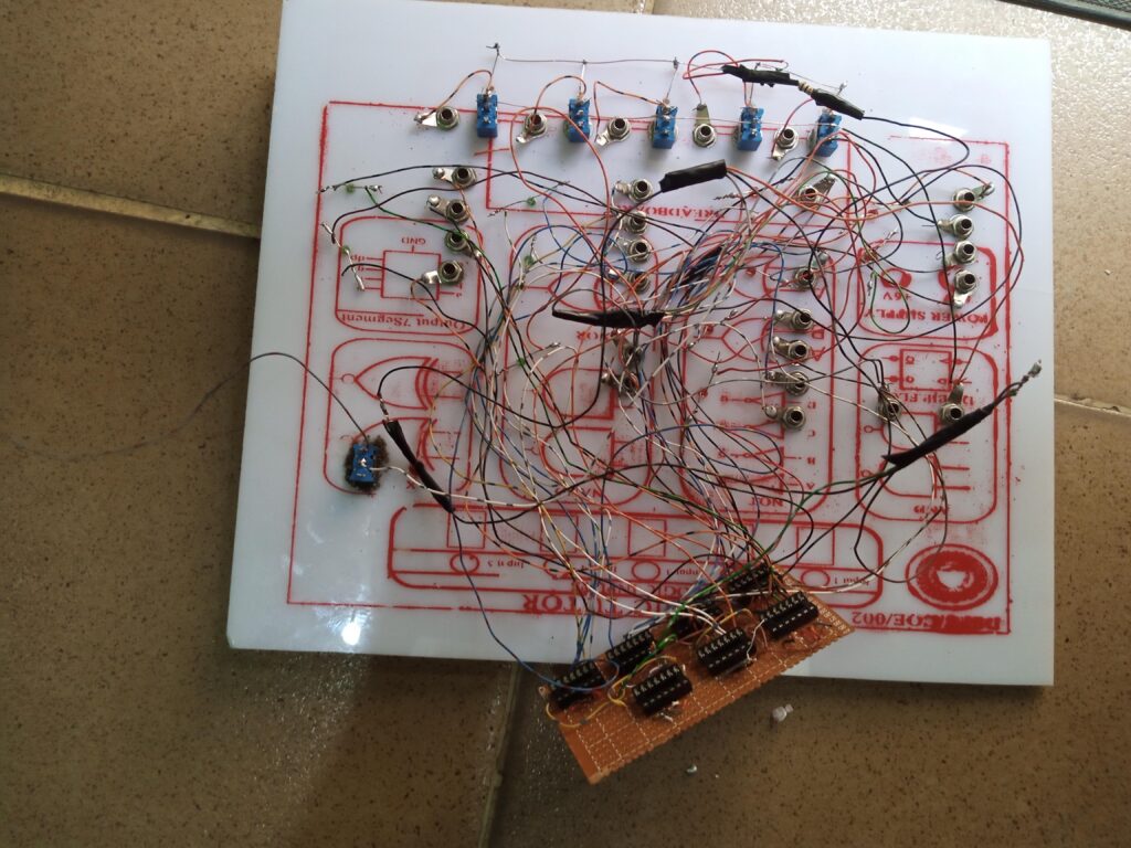
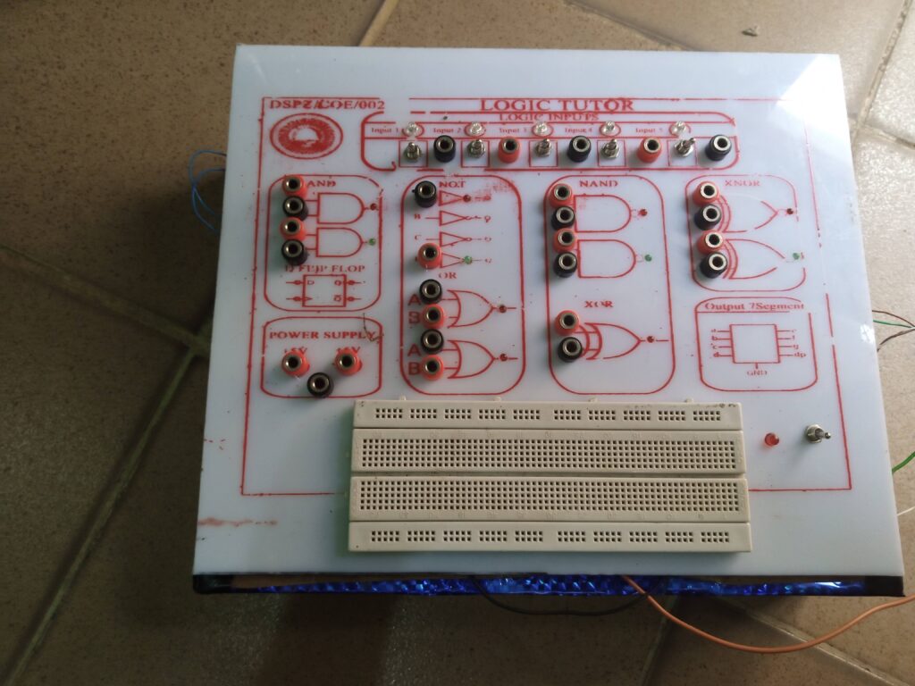
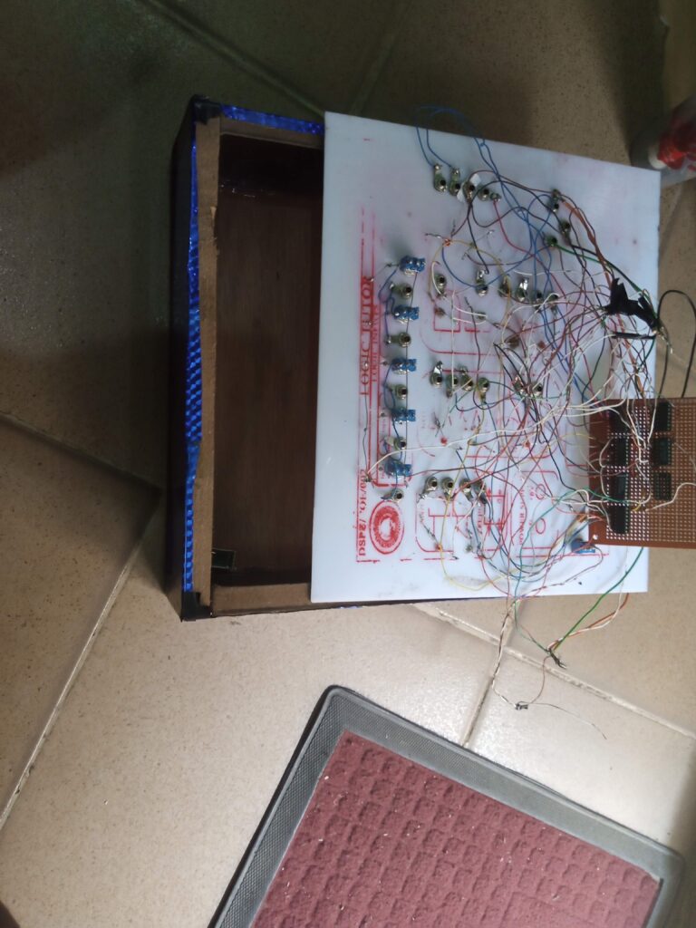

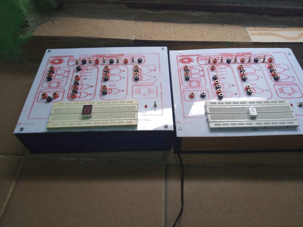
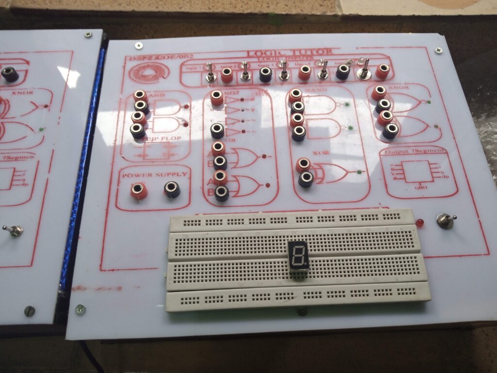
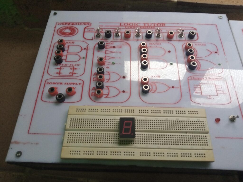
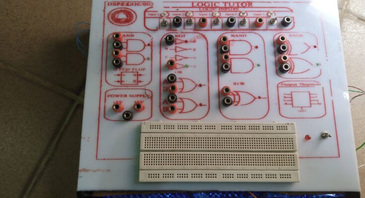
This logic trainer design focuses on using common TTL (Transistor-Transistor Logic) ICs, specifically from the 7400-series, which operate on a +5V DC supply.
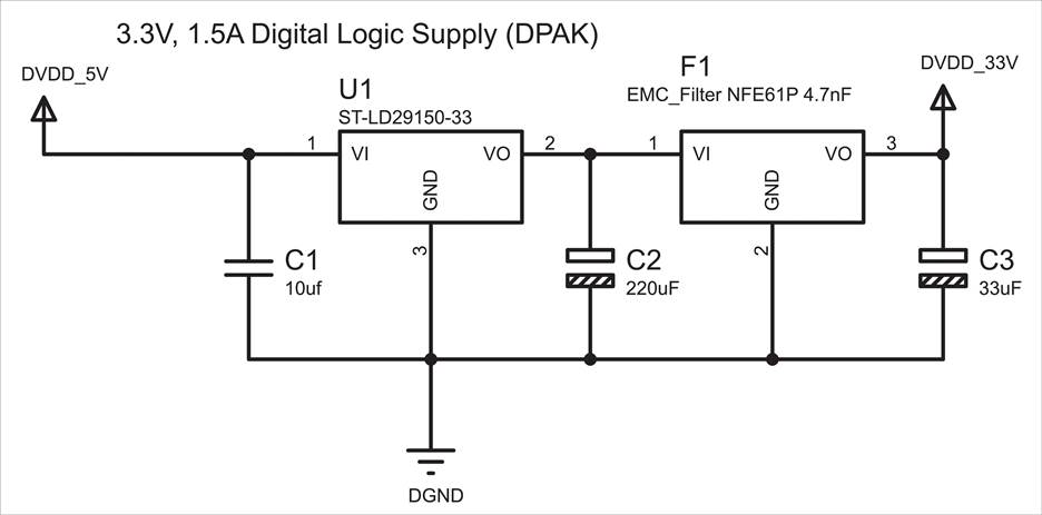
1. Power Supply and Regulation 🔌
The trainer requires a stable +5V supply.
| Component | Number | Function |
| Voltage Regulator | LM7805 | Regulates input voltage (e.g., 9V-12V DC) down to a stable +5V DC output. |
Power Supply Circuit Diagram (Phase 1)
This circuit takes a DC input and ensures a clean, stable +5V output for the logic ICs.
| Pinout (LM7805) | Function |
| Pin 1 (Input) | Connects to the unregulated DC input. |
| Pin 2 (Ground) | Connects to the common ground rail. |
| Pin 3 (Output) | Provides the regulated +5V to the rest of the board. |
2. Logic Inputs (Switches) 🎚️
Simple toggle switches are used, but they must be connected with pull-up or pull-down resistors to ensure a solid logic level (either ‘1’ or ‘0’) is always present at the IC input.
Logic Input Circuit Diagram (Phase 2)
We’ll use a Pull-Down Configuration where the default state is ‘0’ (LOW).
| Component | Function |
| Toggle Switch | Provides HIGH (+5V) or LOW (GND) input. |
| Resistor ($10k\Omega$) | Pull-Down: Connects input to GND to hold it LOW when the switch is open. |

Result:
- Switch ON: Input is connected to +5V (Logic ‘1’).
- Switch OFF: Input is pulled to GND by the resistor (Logic ‘0’).
3. Clock Generation ⏱️
A clock signal is essential for testing sequential logic. The NE555 Timer IC is the standard choice for generating a stable square wave.
| Component | Number | Function |
| Timer IC | NE555 | Configured as an astable multivibrator to generate continuous pulses. |
Astable Multivibrator Circuit Diagram (Phase 3)

| Pinout (NE555) | Function |
| Pin 1 (GND) | Ground. |
| Pin 4 (Reset) | Connected to +V (or Pin 8). |
| Pin 8 (VCC) | Connected to +5V. |
| Pin 3 (Output) | Provides the Clock Pulse. |
| Pin 2 (Trigger) & 6 (Threshold) | Connected together and to the $R_B$-$C$ junction. |
| Pin 5 (Control Voltage) | Bypass capacitor (e.g., $0.01\mu F$) to GND. |

4. Logic Outputs (Indicators) 🚦
Outputs require LEDs, but TTL ICs often cannot supply enough current to drive an LED directly without pulling the output voltage down.
| Component | Function |
| Resistor ($330\Omega$) | Current Limiting: Protects the LED. |
| LED | Visual Indicator: ON for Logic ‘1’, OFF for Logic ‘0’. |
Output Indicator Circuit Diagram (Phase 4)
The LED is typically connected from the +5V rail (VCC) through the current-limiting resistor, and then to the IC output pin.

Operation (TTL Logic):
- IC Output = Logic ‘0’ (LOW): The IC sinks current, completing the circuit path for the LED. LED is ON.
- IC Output = Logic ‘1’ (HIGH): The IC output voltage is near +5V. There is almost no voltage difference across the LED/resistor. LED is OFF.
5. Essential TTL Logic ICs (For Experimentation)
The following ICs should be available for users to wire up on the breadboard area:
| IC Number | Gate Type | Pins | Description |
| 7400 | Quad 2-Input NAND Gate | 14 | Contains four independent NAND gates. |
| 7402 | Quad 2-Input NOR Gate | 14 | Contains four independent NOR gates. |
| 7404 | Hex NOT (Inverter) Gate | 14 | Contains six independent NOT gates. |
| 7408 | Quad 2-Input AND Gate | 14 | Contains four independent AND gates. |
| 7432 | Quad 2-Input OR Gate | 14 | Contains four independent OR gates. |
| 7486 | Quad 2-Input XOR Gate | 14 | Contains four independent XOR gates. |
| 7474 | Dual D Flip-Flop (Positive Edge-Triggered) | 14 | Two independent D-type flip-flops. Essential for sequential logic. |
TTL 14-Pin IC Pinout (Standard Configuration)
Most 14-pin DIP logic ICs share a common power configuration:
| Pin | Function |
| Pin 14 | $V_{CC}$ (+5V) |
| Pin 7 | GND (Ground) |
All other pins are inputs/outputs for the internal gates.
6. Complete Logic Trainer Block Diagram 🗺️
The final design integrates all phases around a central breadboard where users connect the ICs and jumper wires.
